 Graham's Photography Blog & Technical Reviews
Multi Battery Type Lithium Ion Charger
A look at how to construct a simple lithium ion battery charger which has intelligent charging properties and capable of charging a range of batteries like the Sony NPF series, The Panasonic, Canon and Nikon batteries like the BLC12, EL6, EL17 and EL12
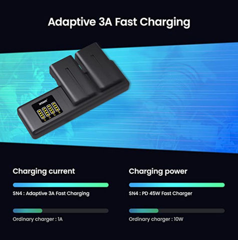
This project was inspired by my review of the XTAR SN4 battery charger that I reviewed recently.
This charger appeared to be ideally suited to this purpose however on full investigation it was flawed in may areas so I decide to try my own alternative construction using components easily available.
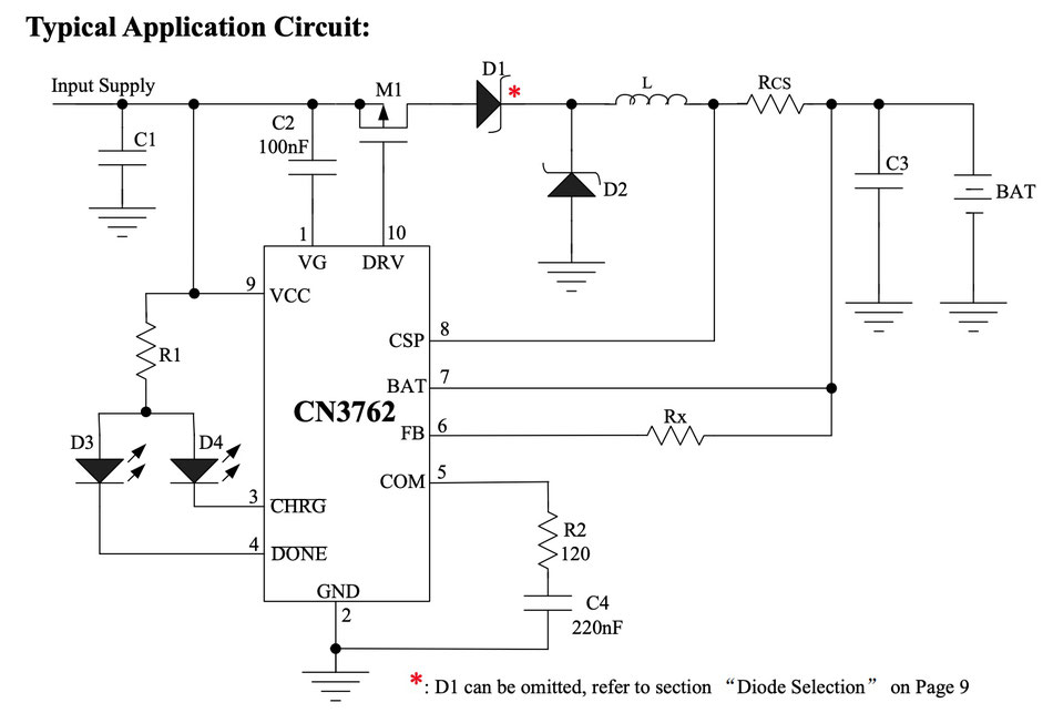
Whilst looking at quite a few commercial chargers that I had in my collection I found one that had the most appropriate charging circuit which used the CN3762 chip.
From the CN3762 product data sheet:
The CN3762 is a constant current, constant voltage 2-cell Li-Ion battery charger controller that adopts PWM
step-down (buck) switching architecture. The charge current is set by an external sense resistor (RCS) across the
CSP and BAT pins. The final battery regulation voltage in constant voltage mode can be adjusted upwards with a
resistor between FB pin and BAT pin; When FB pin is connected to BAT pin directly, the regulation voltage is
8.4V typical with 1% accuracy.
A charge cycle begins when the voltage at the VCC pin rises above the UVLO level and is greater than the
battery voltage by VSLPR. At the beginning of the charge cycle, if the battery voltage is less than 66.5% of
regulation voltage (VREG), the charger goes into trickle charge mode. The trickle charge current is internally set
to 17.5%(Typical) of the full-scale current. When the battery voltage exceeds 66.5% of regulation voltage, the
charger goes into the full-scale constant current charge mode. In constant current mode, the charge current is set
by the external sense resistor RCS and an internal 120mV reference, the charge current equals to 120mV/RCS.
When the battery voltage approaches the regulation voltage, the charger goes into constant voltage mode, and the
charge current will start to decrease. When the charge current drops to 16% of the full-scale current, the charge
cycle is terminated, the DRV pin is pulled up to VCC, and an internal comparator turns off the internal
pull-down N-channel MOSFET at the pin, another internal pull-down N-channel MOSFET at the
pin is turned on to indicate the termination status.
To restart the charge cycle, just remove and reapply the input voltage. Also, a new charge cycle will begin if the
battery voltage drops below the recharge threshold voltage of 95.5% of the regulation voltage.
When the input voltage is not present, the charger automatically goes into sleep mode, all the internal circuits are
shutdown.
An over voltage comparator guards against voltage transient overshoots (>7% of regulation voltage). In this case,
P-channel MOSFET are turned off until the over voltage condition is cleared. This feature is useful for battery
load dump or sudden removal of battery.

The charging diagram of the CN3762 IC
Application Information
Under voltage Lockout (UVLO)
An under voltage lockout circuit monitors the input voltage and keeps the charger off if VCC falls below
6.5V(Maximum).
Trickle Charge Mode
At the beginning of a charge cycle, if the battery voltage is below 66.5% of the regulation voltage, the charger
goes into trickle charge mode with the charge current reduced to 17.5% of the full-scale current.
Charge Current Setting
The full-scale charge current, namely the charge current in constant current mode, is decided by the following
formula:
Where:
ICH is the full scale charge current
RCS is the resistor between the CSP pin and BAT pin
Adjust the Regulation Voltage
If a resistor is connected between FB pin and BAT pin, as shown in Figure 3, the regulation voltage in constant
voltage mode can be adjusted upwards.
Charge Termination
In constant voltage mode, the charge current decreases gradually. When the charge current decreases to 16% of
the full-scale current, the charging is terminated, the external P-channel MOSFET is turned off, no charge
current is delivered to battery any more.
After the charge cycle is completed and both the battery and the input power supply (wall adapter) are still
present, a new charge cycle will begin if the battery voltage drops below 95.5% of the regulation voltage due to
self-discharge or external loading. This will keep the battery capacity at more than 80% at all times without
manually restarting the charge cycle.
Status Indication
The CN3762 has 2 open-drain status outputs: (bar charge) and (bar done). (bar charge) pin is pulled low when the charger is in
charging status, otherwise becomes high impedance. (bar charge)pin is pulled low if the charger is in charge
termination status, otherwise becomes high impedance.
When the battery is not present, the charger charges the output capacitor to the regulation voltage quickly, then
the BAT pin’s voltage decays slowly to recharge threshold because of low leakage current at BAT pin, which
results in a ripple waveform at BAT pin, in the meantime, pin outputs pulse to indicate the battery’s
absence.
The open drain status output that is not used should be tied to ground.
Battery Detection
CN3762 does not provide battery detection function, when the battery is not present, the charger charges the
output capacitor to the regulation voltage quickly, then the BAT pin’s voltage decays slowly to recharge
threshold because of low leakage current at BAT pin, which results in a ripple waveform at BAT pin, in the
meantime, pin outputs pulse to indicate the battery’s absence.
It is generally not a good practice to connect a battery while the charger is running, otherwise the charger may be
in uncertain state, or deliver a large surge current into the battery for a brief time.

I found this in one of my Sony NPF battery chargers by DSTE and it contains the CN3762 IC so I will be sawing this pcb in half (literally) to utilise the DC side which has all the charging connections.
I will be powering each of the charging ports with a USB C to 12volt 2A step up module.
During the teardown of my chargers I came across an extraordinary bad unit, one which should never have been allowed to be sold in my opinion.
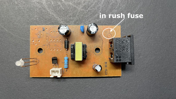
The upper side of the PCB showing where an "inrush" fuse should be fitted.
There should also be some physical separation of the mains input from the switching regulator - such as a slot in the PCB.

The underside of the circuit board showing the way in which the PCB track is actually used as the "fuse".
Should the bridge rectifier or capacitor fail on the input DC side the board may have even caught fire as it is made of the older paper material not a fibre glass type.
No separation of the mains track to the switch mode regulator also is of concern.
The switch mode power supply isn't linked to the output so it effectively just a high frequency transformer to drop the input to around 10v ac on the low voltage side.
regulation for the 8.4v is provided by the 431 IC. So it will drop the charging current through the series resistance and then terminate when the voltage matches the cell voltage at 8.4. This voltage remains across the cell after the end voltage is reached.
Once I have completed to design I will add it here.

The completed project built back into the original case.
the top plate can be interchanged with other types for different batteries.
Input from USB-C PD

The project components using the original 1/2 pcb from the original charger containing the CN3762 chip.
The USB-C PD trigger board ZYX12 is used to provide the 12v at 2A for the charger which will eventually be a dual ganged unit allowing two similar or different batteries to be charged.
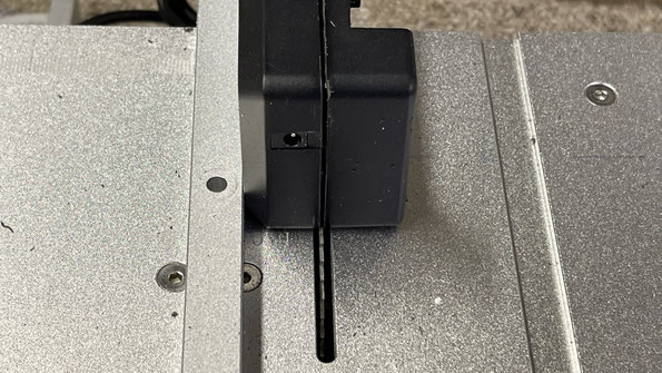
Stage 1 slicing open the original power supply with my miniature table saw.
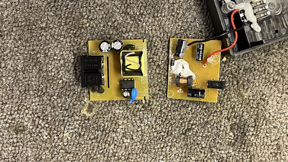
After removing the secondary winding, the XY capacitor and the opto isolator
I cut the board in two.

Testing the charge cut off voltage when charging the attached battery

Cut Off. Charging has stopped and the unit only is using the LED indicator current and no voltage across the battery as it is in standby mode.
Externally Powering Cameras using Power Banks and Lithium Batteries
When you need to use your camera for extended recording times for either video or time lapse you will probably need to use an external power supply. This can be the mains derived ac-dc units if you are using the camera indoors however if you want to use the camera outdoors then you will need to consider some form of a battery based power supply.
In this article I will explore some of the ways in which you can safely power your camera from these battery sources.

The first, and one of the safest ways to provide a higher capacity external power supply is to use one of the higher Sony type NP-F series of batteries along with the battery plate adaptor.
The battery plate has a convenient 1/4-20 mounting option as well as slots for using a velcro strap to attach it to your tripod etc.
This plate is currently unavailable however a similar one is available link
Any of the Sony high capacity batteries can be used like the 750 or 950 types
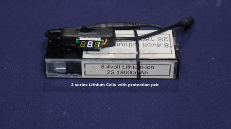
By using two high capacity lithium ion pouch type cells you can construct a very high capacity power source. Using a 2S protection pcb is all that is needed to allow safe charging and discharging facility.
In this example for added physical protection I built the cells into a plastic enclosure and added an external series voltmeter so that I can observe the output voltage.

In the tech talk pages I have often mentioned using standard USB power banks and dc-dc step up convertors to derive the 8.4v for the 5v USB.
Whilst this is a very convenient way to provide the 8.4v you should be aware of a couple of issues with this method.
As the camera does not monitor the usb voltage (it is only displaying the 8.4 output voltage) you must keep a vigilant eye on the power bank capacity remaining. I have had two camera now destroyed as a result of using these power banks left in an unattended time lapse mode.
With some of these power banks when the internal voltage of the lithium cells drops to 3.2 volts the internal circuit shuts down the output 5v.
Some lithium cells start to recover slightly as the load is removed and the power bank again begins to deliver the 5v output. As a consequence the dc-dc convertor now supplies the camera with its 8.4v again. The power bank drops again and the cycle repeats itself. This oscillation can continue until the output is switching on and off frequently enough for the camera to draw too much current from its own internal regulators and probably an internal fuse will blow or the power supplies destroyed.
It is important not to allow the cells in the powerbank not to reach this stage of there discharge and ideally stop them at 25%.
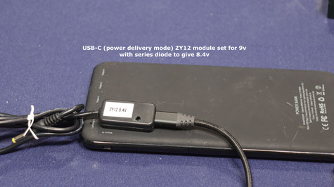
You can use USB-C PD (power delivery) powerbanks to provide power for your camera.
It will only work with PD type c and not the QC (quick charge) circuits.
Once the ZY12 board is programmed to output 9v it is just a case of adding 1 or 2 series silicon diodes to provide 8.4 or 7.8 volts to the camera (I suggest 1N4001 diodes for this purpose).
You just need to build this into a small plastic case for protection.
It is always best to connect this adaptor to the power bank and let it negotiate the programmed voltage (verified by the colour of the LED on the module) and then connect the output to the camera.
The only disadvantage of this method is that if the connection is lost between the power bank and the module you have to re-insert it to start the voltage negotiation phase again to set the 9v output.

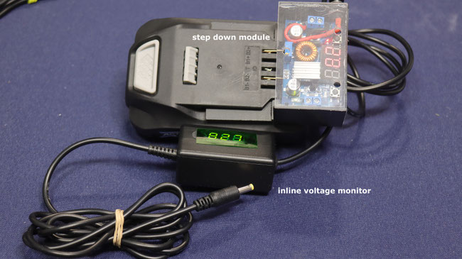
The next option is to use a power tool lithium ion battery pack and a dc-dc step down convertor (buck convertor) to convert from 18/20v to 8.4v
In this example i built the unit into a small enclosure which adds physical protection and a secure way of connecting the board to the battery pack
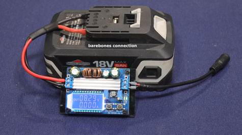
Alternatively you can build a simpler "barebones" module and connect to the battery pack using standard 1/4 inch spade terminals as shown here.
Adjust the output voltage to 8.4 v (6.8 to 8.4 usually is good)
When using the buck convertors it is important to note that with some designs if the internal switching mosfet fails short circuit then the full battery potential will appear at the output terminal and consequence of it possibly damaging the camera which is connected to it.
Also it is advisable to connect the unit to the battery and then connect the camera to the unit as some units when they power up have voltage transients above your set voltage until the reference circuit stabilises the output.
This unit has the facility to monitor both the input and output voltage, output current and output power. There is also a push button switch to switch on/off the output circuit. The IN/ OUT button switches the display of input voltage and output voltage; Long press can switch the display of output current and output power; the ON/OFF button controls the output ON or OFF; Long press can set the default output state of the next power-on to ON or OFF. I recommend setting this to OFF and then switching it on once you see the voltage is at your set level.
The inline voltage monitor shown in the video is just one of the small voltmeter pcb units built into a small plastic box.
It is just a case of cutting the cable and soldering the positive and negative leads to the input terminals of the voltmeter pcb
You could add a small push button or slide switch as well if you wanted to add the functionality of being able to switch of the output to the lead.
I'll have a video shortly on how to make some of the accessories shown in my video such as this unit and the ZY12 USB-C power supply with battery back up.
With any of these switching power supplies there is a slight possibility of power on transients exceeding the voltage that they are set at.
A lot depends upon the adherence to the manufacturers of the switching IC design notes such as the placement of the flyback diode and the use of the correct value low ESR capacitors on the output. For this reason it is always best to have some way of powering up the external power supply and then connecting the output to your camera. This can be as simple as just having the unit unplugged from the dummy battery box and then plugging it in just before you want to use the camera. (simply having the camera in the off position is not a good idea as the camera power supply standby mode is still connected and will be susceptible to these transients).
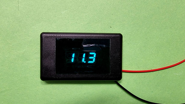
Inline Voltage Meter for Lithium Ion Power Bank Monitoring
The construction of the power bank output voltage monitoring unit

The finished unit attached to my 18,000 mAH power bank
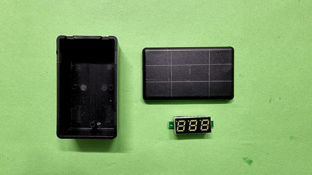
The major components
plastic box approx 50mm x 30mm
the voltmeter PCB
other component 5.5 x 2.1mm extension cable
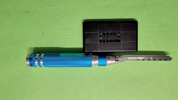
After marking out 24mm x 10mm for the voltmeter drill and cutout the aperture, a file used to clean up the edges.

Glue in the voltmeter pcb, hot glue or "super glue"
optionally add a coloured gel to accentuate the image

Split the 5.5mm x 1.5mm cable and install through plastic grommets in the sides of the plastic box.
Connect all the red wires and all the black wires and solder the joint.

Apply heat shrink insulation over the joints
apply hot glue to secure the cables internally to the grommets.
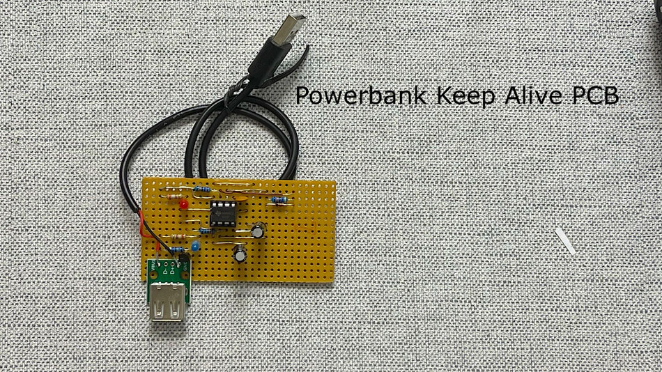
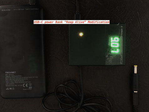
Powerbank Keep Alive Project
Most powerbanks that have a power on/off switch incorporate automatic shutdown when the load current applied is less than some set value.
This means that trying to operate low current devices attached to the powerbanks becomes frustrating as they keep shutting down.
To overcome this I devised the "keep alive circuit" which pulses the output of the powerbank with a load current of between 100 and 150mA.
The time taken to shutdown varies considerably from device to device and also the current limit is also different between devices.
It is best if you can determine the minimum load current that will be tolerated and use this value for the minimum current being pulled by the keep alive circuit.
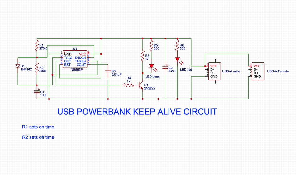
This is the schematic for the keep alive circuit.
Built around the NE555 Timer IC chip. The unit is in the astable oscillator configurations
R1 plus R2 sets the pulse ON time (when C1 charges to 2/3 Vcc) and R2 sets the OFF interval time. (when C1 discharges to 1/3Vcc)
R3 sets the powerbank pulse current drawn and is around 140mA when added to the LED current drive.
The capacitor C1 can be increased or decreased for longer or shorter time frames.
The blue LED indicates when the timer fires and the red LED shows the status of the USB supply.
The input is usually connected by a USB male plug and the output a USB female socket.
The values shown give around 3 seconds on time and 5 seconds off time although changing these values may be needed to satisfy your particular powerbank needs.
If the powerbank has a long shutdown time (say 25-30 seconds) and your load current is under 50mA then the switching to the lower power CMOS version of the 555 timer chip and removing the power on led will help to reduce the standby current of the circuit to a few micro amps giving a longer run time before the powerbank is depleted.
Bluetooth Wireless Remote Control Using The BBC Microbit Controller
Cameras like the Panasonic Lumix FZ200 does not have Wi-fi or bluetooth that can be used to provide a wireless remote shutter release.
This project using the very cheap BBC microbit fulfils that purpose.
It can also be used on other Panasonic cameras as a wireless remote without using a smartphone and the Panasonic Imaging app.

The 2.5mm socket on Panasonic cameras provides a 2 wire interface to enable the wired remote controller to either sense the focus button or the shutter button depressions.
By "shorting an element of the potential divider to ground the camera can determine which button was depressed and perform the appropriate action.
The microbit project uses P0 and P1 to turn on transistors which effectively replace the focus and shutter push buttons.
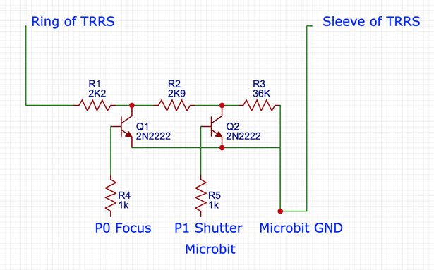
THE CONNECTIONS TO THE MICROBIT

THIS IS THE MICROBIT BLOCK CODE FOR THIS PROJECT

The completed project with the bluetooth remote powered by a lithium coin cell and the receiver at the moment powered by 2 AA
batteries.
To make the receiver smaller I intend to power it also by a 3v lithium coin cell
The "Spectacular" Audio Project
This was my idea to mount a microphone electret condensor capsule adjacent to the hing on the leg of a pair of spectacles.
These condensor mikes are omni-directional and being so close to the sound source would provide sufficient volume for decent audio recordings.
As they move with your head the audio levels remain unchanged as you head moves.
My first proof of concept used electret mics that were originally used in portable cell phones. later versions switched to the in-line mics found on IOS or Android earphone headsets.

The finished project showing the way that the microphone cable is routed from the rear of the earloop.

the mic element from the in-line microphone is attached to the leg of the spectacles using double sided tape and then a section of clear heat sink tubing was then slid over it to provide both mechanical stability and extra protection.
The cable from the mic being routed down the frame and held in place using more clear heat shrink tubing.
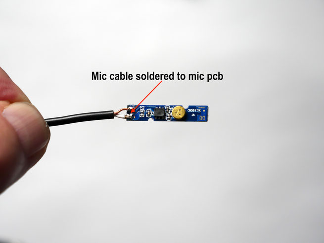
The mic element pcb could be removed from the in-line cable and a new lead soldered to the pcb withe the TRRS or TRS plug depending upon whether the mic was going to be used as a camera input or as a smart-phone accessory.
Modifying the DCC6 Dummy Battery Box to Display Battery Status
The standard DCC6 dummy battery box allows external mains powered adaptors or external lithium-ion batteries to be used with the FZ100, FZ150, Fz80/82 cameras.
When used with the original mains power supply then the battery status is largely irrelevant. However, if you have used an external 8.4v Lithium-ion battery pack then it is important to know what charge is remaining in the battery.
The modification here performs that purpose.

The first stage is to open the battery box.
Do this by inserting a sharp blade in-between the hard plastic base plate and the softer plastic cover.
Work the blade down into the opposite corner to split the ultrasonically welded seam.
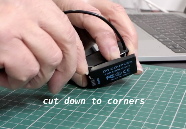
Cut down to the bottom corner on both sides of the battery box.

Remove any "hot-melt" glue from around the PCB
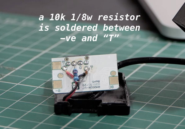
To complete the modification a 1/8w 10K resistor is soldered from the "T" pad to the negative lead connection pad (black wire).
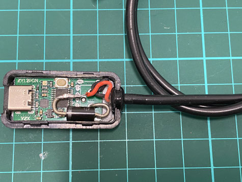
Once that is done re-assemble the box and apply a little drop of "super-glue along the 3 edges. Capillary action will spread the glue along the seams. Wipe off any excess before it dries.

Now when this battery box is used it will display the current charge status of the external lithium-ion battery
USB-C Power Delivery Adaptor for Digital Camera External Power Supply
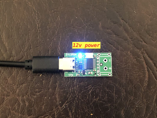
Using a ZY12PDN PCB available on Ebay UK or Amazon.com ( https://amzn.to/37GCuPK ) It is possible to build a USB PD unit to externally power your 8.4v digital camera.

This tiny module provides a means of programming the Power Delivery voltage from the USB-C host device.
It can provide 5v/9v/12v/15v and 19v of voltage with a maximum power of 100W (this will also depend upon the capability of the Host PD device)
The push button is used to set the output voltage. Each depress of the button cycles through the voltages.
It can also be programmed to negotiate a fixed voltage output.
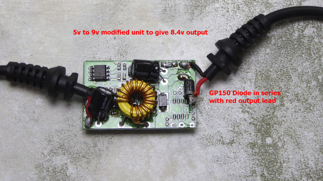
As this unit will deliver 9V at up to 5A (with a suitable host) it can be used to provide the basis of an 8.4volt external power supply if a silicon diode is inserted in the positive output terminal of the device.
This diode will nominally drop 0.6v at typical currents up to 3A.
I chose the 1N5400 as it is capable of 3A continuous current. It would be possible to use a 1N4000 series as in most cases the peak current does not exceed 1.5A with many digital cameras.
This is the completed unit with details of how the 1N5400 diode is connected in the positive output lead of the unit.
The box that I used is from Amazon. https://amzn.to/37DMlpy
The box needs to be filed on the input side to accommodate the USB-C plug.
The PCB is held in place using double side adhesive pad. The output lead is wired to either a 5.5mm x 2.1mm or 4.8mm x 1.7mm plug depending upon the type of socket on the dummy battery box.
the 1N5400 diode https://amzn.to/2N3yzEW
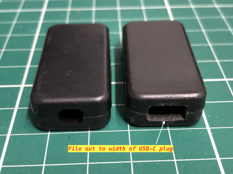
With the suggested plastic case file out one side so that a USB-C plug fits through the aperture.
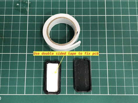
The PCB is held in place by thick foam based double sided tape
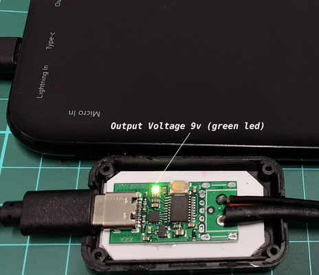
To program this unit to a set output voltage of 9v first disconnect the unit from any power source.
Press and hold the push button down and connect the PD Host.
The LED will flash all colours, release the button and then cycle through the voltages until you reach the one that you require.
You can check the output with a voltmeter or observe the colour of the LED.
For 5V it is RED
for 9V it is GREEN
for 12V it is CYAN
The programming is voltage based and has these steps: 5V, 8-10V, 11-13V, 14-16V, 18-20V, maximum voltage, auto trigger.
By adding a 8.4v lithium ion battery in parallel with the output from the unit (after the series diode) it provides addition current support if needed and also a backup power source if the Host power-bank becomes depleted. At this point this lithium ion battery continues to provide power to the camera. The power-bank can be then exchanged.
If the lithium ion battery becomes partially depleted it will be recharged once this unit is reconnected to the USB-C host again. The usual over voltage/overcurrent and over discharge protection all being satisfied by the battery management board within the lithium ion battery.

An illustration of the ZY12PD board with the series silicon diode and the lithium ion backup battery installed in a small plastic case.
In the latest upgrade of this idea I have included a LED Voltmeter module to draw a slight amount of current from the Host Power Bank.
This 30mA of current is enough to prevent the power bank from going into the sleep mode if there is no load detected.
This is a useful feature as with many cameras going into standby mode this in turn would cause the power bank to go into sleep mode.
It would then be necessary to unplug the ZY12 unit in to wake up the power bank and begin the voltage negotiation sequence again.
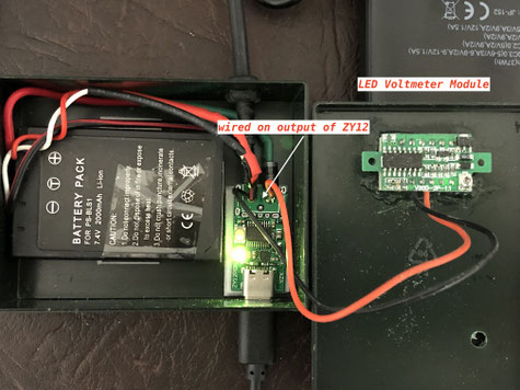
To prevent the onboard lithium-ion battery powering the LED voltmeter when the Host power bank is disconnected it is necessary to wire to voltmeter to the +/- outputs of the ZY12 board.
The in series diode prevents the voltage from going to the LED voltmeter module.
I chose a module which drew sufficient current to keep the host power bank, that I normally use, alive but would have minimal effect on the total output capacity from the unit. Some power banks may require a higher standing current to keep them alive. I suggest increasing the current in steps of about 30mA by adding a parallel resistance of 330 ohm if your power bank still shuts down with this module alone.
If the addition 330 ohm doesn't work try a 150 ohm which would add 60mA to the standby current.
the unit that I used https://amzn.to/2sXLm4X

With just the display wired across the output the standby current taken from the power bank was 20mA

Adding a 390 ohm resistor in parallel with the LED voltmeter increased the standby current to 44mA which was enough to prevent all of power banks that I currently use.
The sequence of connection of the unit is important as the serial data communication has to take place to set the negotiated voltage from the host PD device.
When the unit is plugged into the Host PD device the green led light will illuminate denoting successful connection.
If there is no load on the power bank through this unit the power bank may go into a shut down mode.
If you press the power on button to "wake up" the unit it may not correctly communicate with the ZY12PD board and the LED will flash a white/cyan colour.
Unplug the device and reconnect it to correctly restore communication.
Modifying the Qutaway 5v to 9v Conversion cable for 8.4 Volts
Here you can see the addition of the GP150 silicon diode (or a 1n54 series diode) connected in series with the red lead.
De-solder the red lead from the pcb, insert the diode with the anode (plain end marking) to the pcb and then connect the red cable to the cathode (ringed end) of the diode.
Ensure the diode is clear of the pcb when installed.
Re-fix the covers and add suitable marking to the unit to designate it now to be 8.4 volt output.
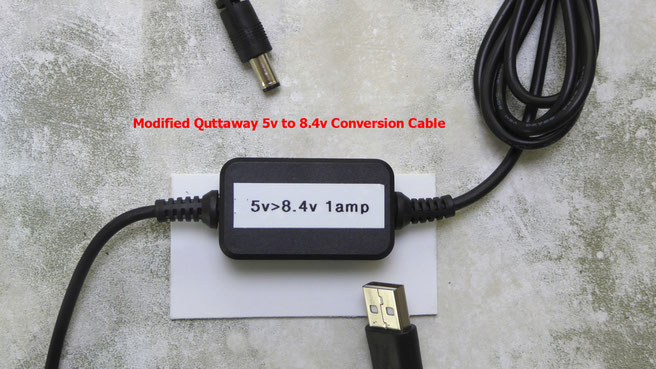
The completed unit.
Amazon link for module
Amazon UK http://amzn.to/2w34ZW5
Amazon USA http://amzn.to/2u1w52s

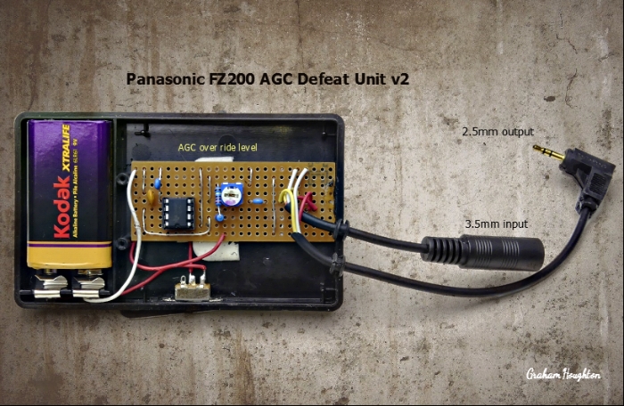
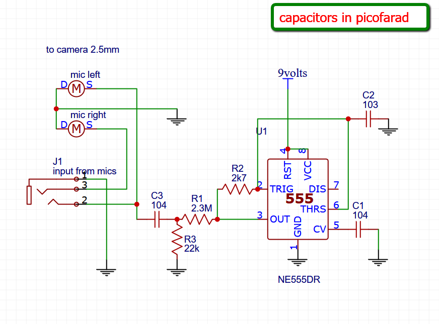
Schematic for the working version of the FZ200 AGC Defeat Unit
The final circuit turned out to be more simplistic than I had originally thought.
I assumed that the input would need to be a sine wave to prevent harmonic distortion if a square or triangular wave was used for the input to the camera. In testing I found that the camera would still perform well with a square wave input so I decide to try both an astable multi-vibrator pair of transistors running at 20 KHz and a NE555 timer IC.
In the end I decide to use the more stable 555 IC as the frequency remained solid even during the battery run down.
Here is the schematic for the project.
The timing is done by R2-C2 giving 20KHz. The output from pin 3 is attenuated by R1-R3 to 7-8millivolts at the camera input after being coupled with the mic input and allowing for its impedance.
the right hand mic input goes straight to the camera input whilst the left hand input has the 20KHz signal injected into it.
If you wanted to get finer control of the AGC defeat voltage input R3 could be substituted with a 27K resistor and a 100K potentiometer in parallel with it. The output would be taken to C3 form the wiper of the pot. This would allow the output to be set for 0V to about 10millivolts.
The unit is powered by a PP3 9v battery.
Here is the built unit. I used a stereo splitter cable from £/$ store to get the wired 3.5mm inline socket. The 2.5mm plug I wired but again it could be obtained from a 2.5mm to 3.5mm audio cable if you didn't want to have to solder one up.
The version 2 of this unit now features a trim pot (22K) in place of R3 ( the wiper connects to C3) so that you can adjust the level of the bias signal sent to the FZ200. Adjust to about 1/3 or the rotation as a starting point. Do a test recording with the unit on and adjust the trim pot until the background noise doesn't increase when you stop talking.

Audio Line Level to Microphone Level Variable Attenuator
A simple voltage divider circuit to provide 20dB (x100) reduction of voltage from the nominal 500mV line output voltages to the 5mV microphone input voltages of smartphones, cameras and audio recorders.

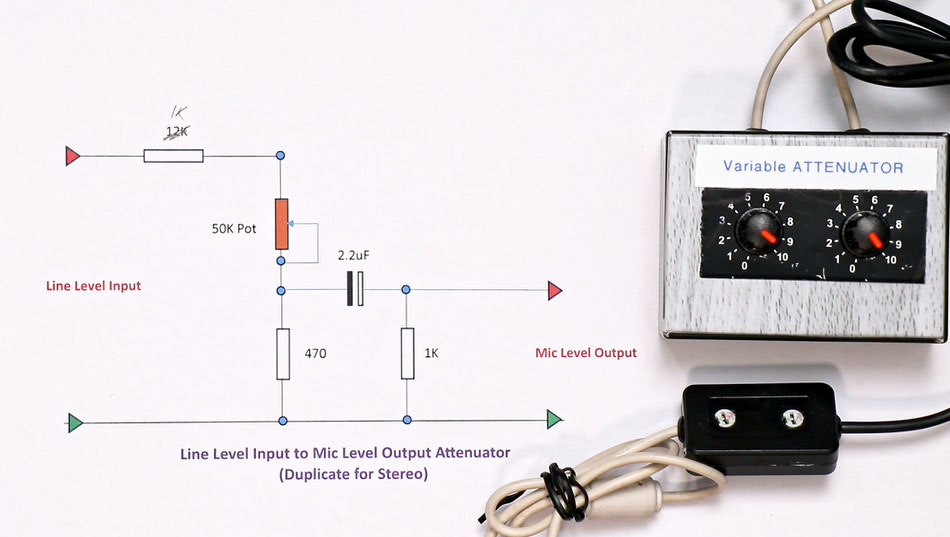
Two versions of the device. The lower unit has trim pots, adjustable with a small screwdriver, but provides the same functionality in a much smaller package.
The circuit provides a potential divider chain of the 50K potentiometer and the 470 ohm resistor/ The series 1K resistor on the input provides current limiting from the output device if the potentiometer is set to its minimum resistance position.
The 2.2uF capacitor provides DC isolation of any mic input circuit which may have microphone bias voltages present.
The 1K output resistor provides load recognition when used with some smartphones which require to "see" under 2K on their inputs.
Wiring to and from the unit should be made with screened to reduce the possibility of electrical noise being induced.
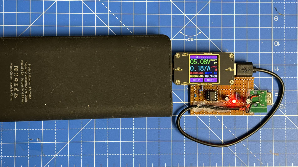
Higher Current Version of Power Bank Keep Alive Circuit
I recently started to use higher capacity power banks for some projects and found that these would not stay active using the original design of my keep alive (featured on this page). Testing these units with an electronic load I found that most of these required in the order of 160mA to defeat the power down circuit within the power banks and needed to pulse for about 2 seconds as well. The shut down time was also quite short (as little as 8 seconds in one unit).
So I re-designed the circuit to trigger the units more frequently and apply a 200mA pulse, which when added to the circuit under load, kept the power bank from shutting down.
So here is the updated design.

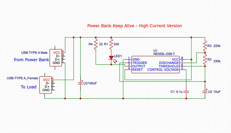
The input to the unit is now using a USB-A power lead with the micro usb plug cut off. This prevents stress on the socket of the power bank and is a little easier to use that the mk1 version.
Basically the 555 timer is wired as an ASTABLE oscillator and the charge time of the timing capacitor (U2) is determined by the sum of R2 and R3 . Once the 2/3Vcc threshold is reached at pin 6 the 555 starts to discharge the charge on U2 through R2.
When the voltage falls to 1/3 Vcc the 555 flips to charging mode again.
During charging the output on pin 3 is held at Vcc and during discharge pin 3 can either sink or source a current of up to 200mA.
R4 provides the pulse load plus a small 20mA current of the LED which is used to indicate the circuit operation.
U3 adds some decoupling to the power supply. and C1 is used for decoupling the 555.
The approximate timings can be calculated from High = 0.693(R3 + R2)C1 and Low = 0.693 R2xC1 which gives 3.8 seconds High (OFF) and 2.3 seconds Low (ON)
2 Cell Lithium Ion Battery Pack for Cameras

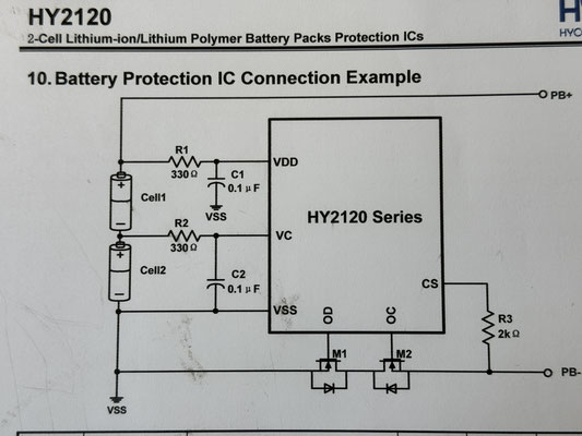
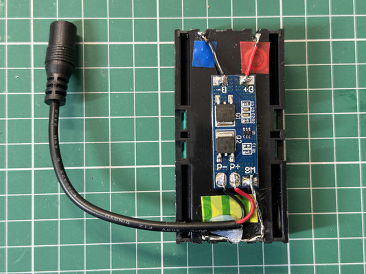
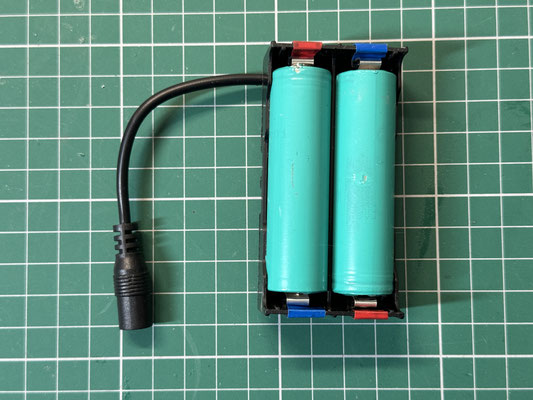
This simple build utilises a 2 cell battery box, 2 lithium 18650 cells, a 2 cell protection PCB and a 5.5 x 2.1 wired socket.
The heart of the project centres on the HY2120 protection IC which constantly monitors the status of the voltage on cell1 and cell2. If they are within the range of the voltage from the over discharge to overcharge states then the outputs OC and OD are enabled high to turn on the two Mosfets which are in series with the negative battery rails.
YouTube Video
Parts used, Affiliate links on Amazon UK.
2 cell battery box: https://amzn.to/3PlCOfl
Lithium Ion cells: https://amzn.to/3IcOyfQ
Protection PCB: https://amzn.to/3UVUx0i
5.5x2.1 socket: https://amzn.to/3Vdb4NJ
From the datasheets
11.1. Normal Status
This IC monitors the voltage of the battery connected between the VDD pin and VSS pin and the
voltage difference between the CS pin and VSS pin to control charging and discharging.
When the cell1 and cell2 voltage is in the range from over discharge detection voltage (VDLn) to
overcharge detection voltage (VCUn), and the CS pin voltage is in the range from the charge
overcurrent detection voltage (VCIP) to discharge overcurrent detection voltage (VDIP), the IC turns
both the charging and discharging control MOSFET on. This condition is called the normal status.
Under this condition, charging and discharging can both be carried out freely.
Notice: Discharging may not be enacted when the battery is first time connected. To regain
normal status, CS and VSS PIN must be shorted or the charger must be connected.
11.2.1 Overcharge release code 1 model
The normal state of the battery voltage between VDD pin and VC pin (the voltage of Cell 1) and the
voltage between VC pin and VSS pin (the voltage of Cell2), if either voltage becomes equal or more
than the overcharge detector voltage (VCUn), and continued exceed overcharge delay time (TOC) an
external charge control Nch MOSFET turns off with OC pin being at "L" level.
To reset the overcharge and make the OC pin level to "H" again after detecting overcharge, in such
conditions that a time when the both Cell1 and Cell2 are down to a level lower than overcharge
voltage, by connecting a kind of load to VDD after disconnecting a charger from the battery pack.
Then, the output voltage of OC pin becomes "H", and it makes an external Nch MOSFET turn on,
and charge cycle is available. In other words, once overcharge is detected, even if the supply
voltage becomes low enough, if a charger is continuously connected to the battery pack, recharge is
not possible.
11.3. Overdischarge Status
11.3.1. Products with Power-down Function
Batteries under normal operation mode, voltage of cell 1 that connected to VDD and VC pin or voltage
of cell 2 that connected to VC and VSS pin drops lower than over discharge detection voltage (VDLn)
and the mode continues longer than over discharge detection delay time (TOD) during discharging,
HY2120 series will turn the OD pin output voltage from high level to low level and turn the discharging
control MOSFET off (OD pin) so as to stop discharging. This condition is called the “Over discharge
Status”.
When MOSFET is off, CS pin voltage is pulled up by IC internal resistor to VDD, reducing IC power
consumption value to that of in the sleep mode (<0.1uA). This condition is called the “Sleep Mode”.
The over discharge status will be leased by two following cases. OD pin output voltage turns from low
level to high level, conducting discharge control MOSFET.
(1) If CS pin voltage lowers than charge overcurrent detection voltage (VCIP) when charger is
connected, voltage of cell 1 and cell 2 goes higher than over discharge detection voltage (VDLn), the
over discharge status is released and back to normal operation mode.
(2) If CS pin voltage is higher than charge overcurrent detection voltage (VCIP) when charger is
connected, voltage of cell 1 and cell 2 goes higher than over discharge release voltage (VDRn), the
over discharge status is released and back to normal operation mode.
11.5. Charge Overcurrent Status
When CS pin voltage lowers than charge overcurrent detection voltage (VCIP) and this status lasts
longer than charge overcurrent delay time (TCIP) during charge process of batteries under normal
operation, OC pin voltage output will change from high potential to low potential. At this time,
MOSFET (OC pin) is disabled and charge stopped. This status is called “Charge Overcurrent
Status”.
If CS pin voltage increases higher than charge overcurrent detection voltage (VCIP) by disconnecting
charger after enter charge overcurrent status, the charge overcurrent status will be released and
restore to normal operation mode.
Updated Microcontroller Based Powerbank Keep Alive Device
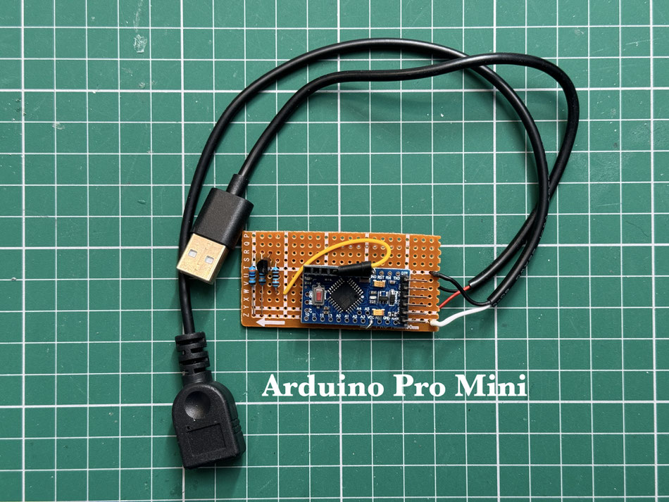
Using inexpensive Arduino Pro Mini a simple device with 3 output choices to allow for power banks with longer shutdown times.
The lead can be plugged into port 5,6 or 7 to give times from 18 seconds to 25 seconds and pulsed for 500msec at 200mA.
Because of the 20mA limit on the microcontroller pins a 2N2222 transistor is used to provide the current pulse across the USB rails.
Here is the suggested code:
#define Trigpin1 6 // physical pin numbers assigned here equated to D6,D7, D8 and built in Led pin D13
#define Trigpin2 7
#define Trigpin3 8
#define Trigpin4 13 // only used for diagnostics - built in LED
void setup() {
// initialise digital pins as an outputs here.
pinMode(Trigpin1, OUTPUT);
pinMode(Trigpin2, OUTPUT);
pinMode(Trigpin3, OUTPUT);
pinMode(Trigpin4, OUTPUT);
}
// the loop function runs over and over again forever
void loop() {
Dlay1(); // call these subroutines
Dlay2();
Dlay3();
}
void Dlay1() { // the first port with about 18 seconds total delay
digitalWrite(Trigpin1, HIGH); // turn the LED on (HIGH is the voltage level)
delay(500); // wait for a second
digitalWrite(Trigpin1, LOW); // turn the LED off by making the voltage LOW
delay(8000);
} // 8.5 seconds
void Dlay2() {
Dlay1(); // pulse pin 6 again
digitalWrite(Trigpin2, HIGH); // turn the LED on (HIGH is the voltage level)
delay(500); // wait for a second
digitalWrite(Trigpin2, LOW); // turn the LED off by making the voltage LOW
delay(500);
} // total 9.5 seconds
void Dlay3() {
Dlay1(); // pulse pin 6
Dlay2(); // pulse pin 7
digitalWrite(Trigpin3, HIGH); // turn the LED on (HIGH is the voltage level)
delay(500); // wait for a second
digitalWrite(Trigpin3, LOW); // turn the LED off by making the voltage LOW
delay(500);
} // total 19 seconds